Silicon Photonics Wafer-Level Testing — Accurately Reflecting Silicon Photonics Chip Performance
The demand for greater bandwidth at every stage of wired and wireless communications, combined with rising data center speeds, is pushing the industry away from copper interconnects toward silicon photonics.
Silicon photonics leverages the mature CMOS process platform to generate, modulate, transmit and detect optical signals on a silicon substrate, offering inherent advantages of high bandwidth, low power and high integration. As 400G, 800G and even 1.6T optical modules enter commercial deployment, silicon photonics chips are moving from the lab to large-scale production, placing unprecedented demands on wafer-level testing.
Challenges & Solutions
Industry Pain Points
- Silicon photonics chips demand precise optical-electrical coupling; conventional probes cannot perform both tests simultaneously.
- Poor probe contact repeatability in wafer-level testing leads to inaccurate yield assessment.
- High insertion loss at high frequencies affects optical modulator performance verification.
Our Advantages
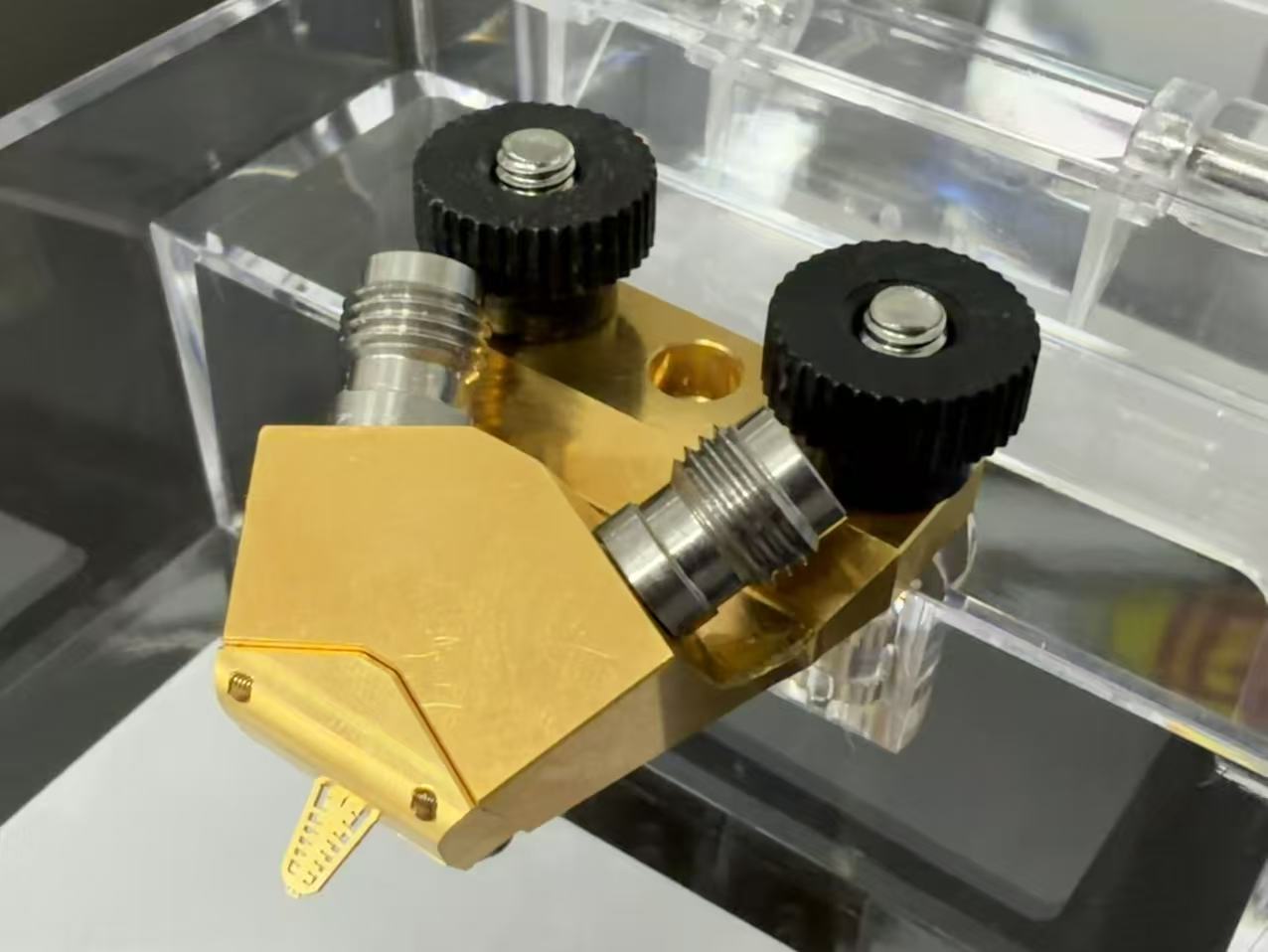
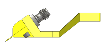
- Probes designed for silicon photonics chips support signal testing from DC to 110 GHz.
- High-precision MEMS process with contact repeatability better than 0.05 dB ensures consistent wafer-level testing.
- Ultra-low insertion loss (below 1.5 dB) preserves signal integrity to the maximum.
Jinwei's silicon photonics test solutions seamlessly integrate electrical and optical testing, helping customers precisely screen performance at the wafer stage and accelerate product iteration.